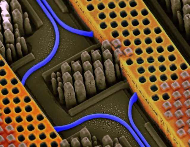
IBM has announced that it is ready to mass produce a new class of computer chips that utilize both copper and optic fiber routing of information on the same computer chip. A single CMOS-based nanophotonic transceiver is capable of converting data between electric and optical with virtually no latency, handling a data connection of more than 25 gigabits per second. Depending on the application, hundreds of transceivers could be integrated into a single CMOS chip, pushing terabits of data over fiber-optic connections between processors, memory, and storage systems optically over distances ranging from two centimeters to two kilometers. Here is the press release:
On December 10, 2012 IBM announced a breakthrough optical communication technology which has been verified in a manufacturing environment. The technology – called “silicon nanophotonics” – uses light instead of electrical signals to transfer information for future computing systems, thus allowing large volumes of data to be moved fast between computer chips in servers, large data-centers, and supercomputers via pulses of light.
The technology breakthrough allows the integration of different optical components side-by-side with electrical circuits on a single silicon chip, for the first time, in standard 90nm semiconductor fabrication. The new features of the technology include a variety of silicon nanophotonics components, such as modulators, germanium photodetectors and ultra-compact wavelength-division multiplexers to be integrated with high-performance analog and digital CMOS circuitry.
The use of a standard chip manufacturing process will alleviate high cost of traditional interconnects. Single-chip optical communications transceivers can now be manufactured in a standard CMOS foundry, rather than assembled from multiple parts made with expensive compound semiconductor technology.
Furthermore, dense integration of optical circuits capable of transmitting and receiving at high data rates will solve the limitations of congested data traffic in current interconnects. IBM’s CMOS nanophotonics technology demonstrates transceivers to exceed the 25Gbps data rate. In addition, the technology is capable of feeding a number of parallel optical data streams into a single fiber by utilizing compact on-chip wavelength-division multiplexing devices. The ability to multiplex large data streams at high data rates will allow future scaling of optical communications capable of delivering terabytes of data between distant parts of computer systems.

I wonder how long it will take these new chips to become integrated into data centers and how long it will take them to find their way into consumer devices.


0 comments :
Post a Comment